The main wafer cutting technologies at present are scribing and sawing. The problem is that fragments and gouges will form along the broken edges of the grains, and cracks will form and spread from the edges of the grains into the substrate, rendering the integrated circuit invalid.
The use of plasma contactless processing can effectively solve the problem of wafer cutting with thin wafers within 50um and fine pitch wafers within 10um.
(1) Initial stripping can be performed using a multi-step laser scribing process to strip through the mask layer, through the wafer scribe line (including the metallization layer) and partially into the silicon substrate.
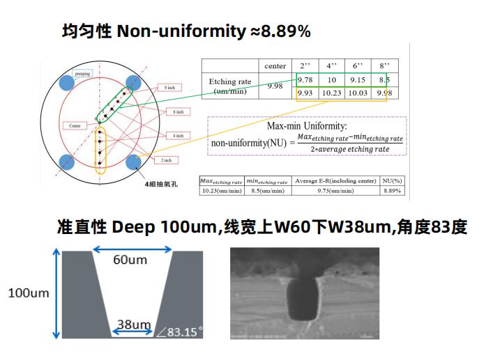
(2) Perform subsequent through-silicon deep plasma etching to complete the singulation of the chip.


