Suzhou Takchip Semiconductor Co., Ltd.
Plasma Etching

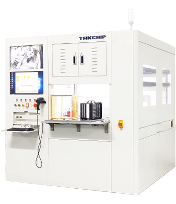
TKP-500W

Fully automatic wafer plasma etching equipment
Takchip TKP-500W fully automatic wafer plasma cleaning/etching equipment is mainly used for wafer surface cleaning and pretreatment, and is compatible with 6/8/12-inch wafers. TKP-500W is mainly composed of 6/8/12-inch wafer loading port, dual-arm wafer robot, aligner and vacuum chamber module, which can provide effective solutions for wafer debonding and hole cleaning, wafer adhesion enhancement, metal oxide removal and wafer stress release.
Fully automatic wafer plasma etching equipment
ADVANTAGES & FEATURES
  • High performance power system
    High-performance plasma power system ensures uniformity of erosion and activation.
  • Compatible with multiple wafer sizes
    The equipment is compatible with 6-inch, 8-inch and 12-inch wafers to meet flexible production needs.
  • Plasma treatment uniformity
    Fully automatic plasma chamber design, process optimization, reasonable plasma reaction space and uniform treatment.
  • Reduce the risk of wafer damage
    Equipped with a high-precision dual-arm wafer robot to accurately position the wafer and reduce the risk of wafer damage.
  • Reduce the risk of wafer damage
    The integrated control system design simplifies the operation process, lowers the application threshold, and improves production efficiency.
application

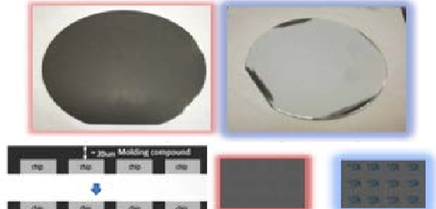
EMC dry etching

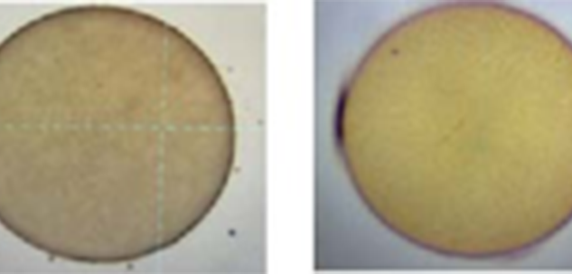
Plasma glue removal
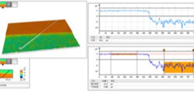
Si, SiC, ABF, metal micro-etching
Wafer plasma cleaning

application
Project Content
Equipment size 1900*1500*2100mm(L*W*H)
Cavity Mode Side opening
Wafer size 8 inches (compatible with 6 inches, 12 inches) thickness ≥ 200um, warpage ≤ 1mm
Power Configuration RF1000W、13.56MHz
Process Gas O2, Ar, N2, CF4 (spare)
Air intake method Top air intake
Flow Meter 0-300sccm
Vacuum Pump Dry Pump
Vacuum degree 0.02Torr
Copyright © Suzhou Takchip Semiconductor Co., Ltd. All rights reserved SuICP No. 2024094040-1 Web design