Suzhou Takchip Semiconductor Co., Ltd.
Trench & Drilling

TKP-300L

Fully automatic laser cutting slotting & drilling
Takchip TKP-300L fully automatic laser marking equipment is mainly used for laser marking processing in the field of IC packaging. TKP-300L is mainly composed of automatic loading and unloading mechanism, visual inspection mechanism, marking positioning mechanism, 2D code reading mechanism, cleaning and dust removal mechanism, etc. Through quick and easy adjustment, the equipment can handle workpieces with a width of 50-100mm and a length of 160-300mm, and adapt to the marking needs of semiconductor devices, lead frames, substrates and tray units made of metal, plastic, ceramic, glass and other materials.
Fully automatic laser cutting slotting & drilling
ADVANTAGES & FEATURES
  • Multi-size compatibility
    Strong compatibility, adapting to workpieces of various sizes and shapes (50-100mm wide, 160-300mm long).
  • High precision and high reliability
    The marking has high precision, fast speed and good stability, meeting the needs of high-quality continuous production.
  • Independent research and development of the whole machine
    Independently develop equipment software and hardware systems to ensure stable and smooth operation of the equipment and more convenient maintenance.
  • Compliant with semiconductor standards
    Support SECS/GEM, two-year log traceability; with processing report, alarm indication and solution prompts and other functions.
  • Automation and high efficiency
    The equipment is fully automatic in production, has high processing efficiency, and has product traceability capabilities.
Advanced packaging special-shaped cutting

It can be applied to advanced packaging cutting including SIP, Fanout, and 3D.

Such as A/H watch special-shaped cutting, Apple TWS earphone cutting, fingerprint module, camera module, automotive electronic module, SD card, PCB/FPCB/PI film cutting; EMC cutting/grooving; QFN cutting/grooving/filling

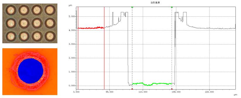
Laser drilling (TMV)

The laser drilling process can form vias on plastic packaging or silicon materials to achieve three-dimensional packaging of multi-layer chips.

The shape/size or aspect ratio of the vias can be controlled by controlling the characteristics of the laser drilling process (eg, power, area, duration, etc.).
application

EMC Marking Samples

L/F labeled samples

FPCB marking sample

Copyright © Suzhou Takchip Semiconductor Co., Ltd. All rights reserved SuICP No. 2024094040-1 Web design