

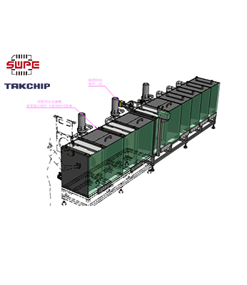


|
Application |
Copper pillar |
Fine Line |
Blind hole |
|
|
Result |
|
|
|
|
|
Ability |
5 & gt; Depth to width ratio& gt; 2 (Production line verification / No jump plating) Electroplating rate:; 10~15 ASD (According to the ability of the potion) Uniformity of the entire board& lt; 10% (Patent Depended) |
2 x 2 um / 8 x 8 um / 15 x 15 um
Uniformity of the entire board& lt; 10% (Patent Depended) |
Depth to width ratio>& nbsp;2 ; Minimum 20x20 um Dimple & lt; 10um Uniformity of the entire board& lt; 10% (Patent Depended) |
|
The same hardware design can be applied to different processes
The same process can be applied to different liquid medicine suppliers, which is beneficial for customers to choose the lowest operating cost
|
Application |
Blind hole |
Through-hole |
Through-hole filling |
|
Result |
|
|
|
|
Ability |
Dimple & lt; 10um
Uniformity of the entire board < 10% (Patent Depended)
|
AR > 16 ( AR 18/20 on going) 4 ASD w/ 80% DC Only |
AR > 3 DC only |


