Suzhou Takchip Semiconductor Co., Ltd.
Inline Sputter

TKP-0602S

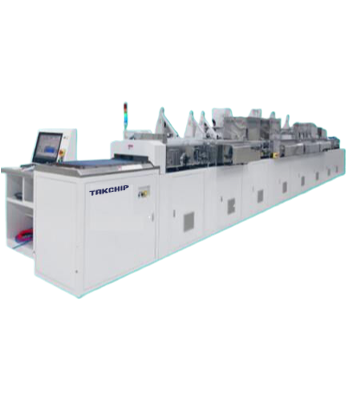
Continuous Vacuum Sputtering System
Takchip SUPREME continuous vacuum sputtering system is mainly used for SiP EMI electromagnetic shielding layer deposition, Fanout RDL seed layer deposition, NPL layer deposition and BSM wafer back metallization deposition, and is suitable for efficient batch processing of large-size workpieces. SUPREME is mainly composed of loading and unloading chambers, plasma chambers, buffer chambers, sputtering process chambers, etc. Different chamber designs can be provided according to different product application requirements. The deposited film has high uniformity, high hole/sidewall coverage, high adhesion and other performance characteristics.
Continuous Vacuum Sputtering System
ADVANTAGES & FEATURES
  • High film uniformity
    The deposited films have the performance characteristics of high uniformity, high hole/sidewall coverage, and high adhesion.
  • Low process temperature
    The sputtering technology used has a low process temperature, which effectively reduces the risk of thermal damage to the substrate
  • Many types of materials
    Various types of thin films can be deposited on a variety of substrate materials such as ABF/EMC/PID, and are widely used.
  • High production efficiency
    It is suitable for efficient batch processing of large-size workpieces, improves production efficiency and meets high production capacity requirements.
  • Personalized configuration
    Customized chamber design enables personalized configuration of the sputtering system to meet specific production needs.
application
Project Content
Equipment size 1920*1320*1820mm(length*width*height)
Radio frequency power supply RF1000W,13.56MHz
Vacuum chamber Stainless steel
Vacuum line Stainless steel pipes
Process Gas Ar, 0z optional
Control System PC
Copyright © Suzhou Takchip Semiconductor Co., Ltd. All rights reserved SuICP No. 2024094040-1 Web design